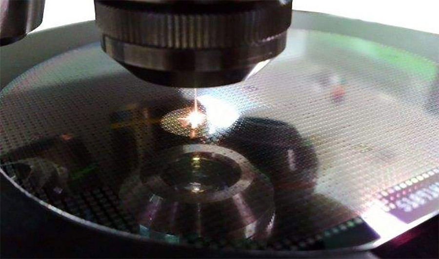
As another great invention after atomic energy, computer and semiconductor since the 20th century, laser has gradually made breakthroughs in the semiconductor manufacturing process. The well-known laser marking makes the fine semiconductor chip identification a very simple job. Laser-cutting semiconductor wafers has become a major force in semiconductor wafer cutting by changing the drawbacks of conventional contact-type cutter wheel cutting.

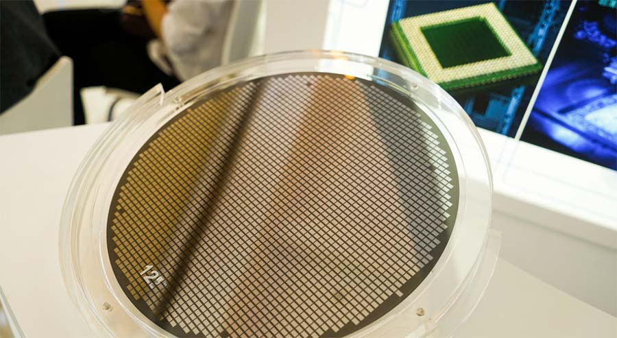
Wafer dicing is an indispensable process in the manufacturing process of semiconductor chips, and it is a downstream process in wafer fabrication.
In the wafer dicing industry, there are two main cutting processes, one is traditional blade cutting, and the other is a new type of modern process laser dicing. Below, the advantages of laser scribing will be demonstrated by comparing the two cutting processes.

Blade dicing
The earliest wafers were diced (cut) with a dicing system, and this method still occupies a large share of the world's chip-cutting market, especially in the field of non-integrated circuit wafer dicing. The diamond saw blade (grinding wheel) dicing method is a common wafer dicing method.

Problem
● The scriber directly acts on the surface of the wafer to cause damage inside the crystal, which is prone to wafer chipping and wafer damage;
● The blade has a certain thickness, which results in a larger scribe line width of the tool;
● The consumables are large, and the blades need to be replaced every half month;
● The environment is polluted, and the silicon powder after cutting is difficult to handle.
Laser scribing
Laser scribing is the use of high-energy lasers to focus the spot to cut the wafer material. Since the focused spot can be as small as sub-micron, it is very delicate in the process of processing the wafer.
Processing advantage
● The laser has little influence on the electrical properties of the chip and the yield is high;
● Laser dicing processing speed block, up to 150mm / s;
● Laser can easily cut wafers of different thicknesses
● The laser can cut more complex wafer chips, such as hexagons;
● Laser dicing non-contact cutting has less damage to the substrate
| Scribing equipment | Raditional dicing method (grinding wheel) | Laser dicing method (light) |
| Cutting speed | 5-8mm/s | 1-150mm/s |
| Cutting line width | 30~40 microns | 30~45 microns |
| Cutting effect | easy to collapse, broken | smooth and not easy to break |
| Heat affected zone | large | small |
| Residual stress | large | Very small |
| Wafer thickness requirements | More than 100 um | no thickness requirement |
| Adaptability | Different types of wafers need to be replaced | Can adapt to different types of wafers |
| With or without loss | Need to remove ionized water, replace the tool, the loss is large, | the loss is very small |
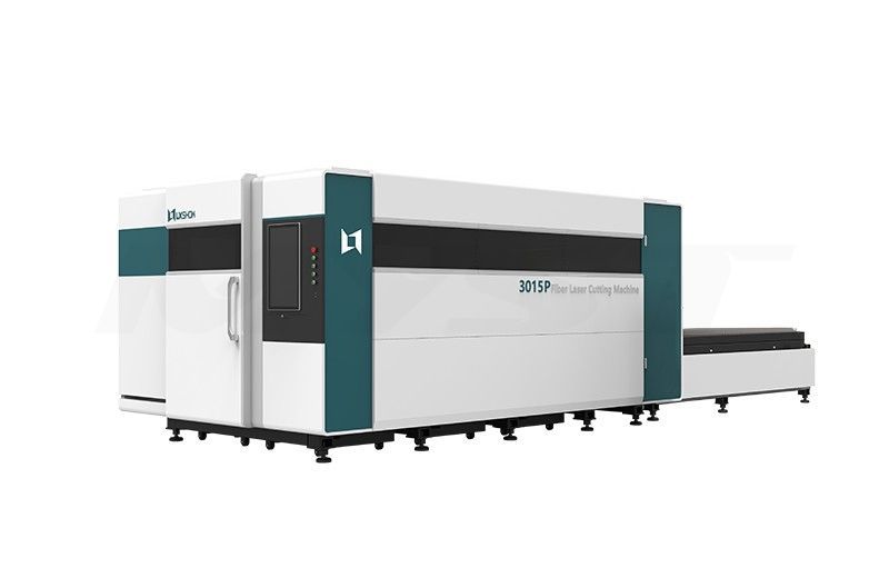
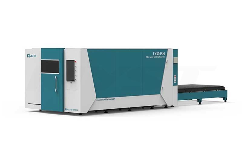
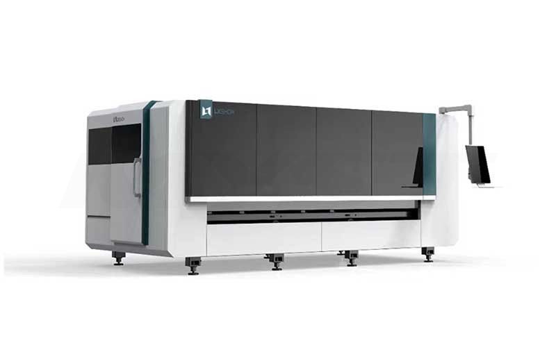
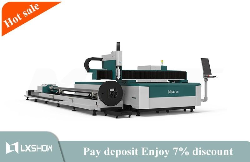
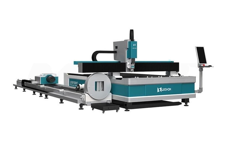
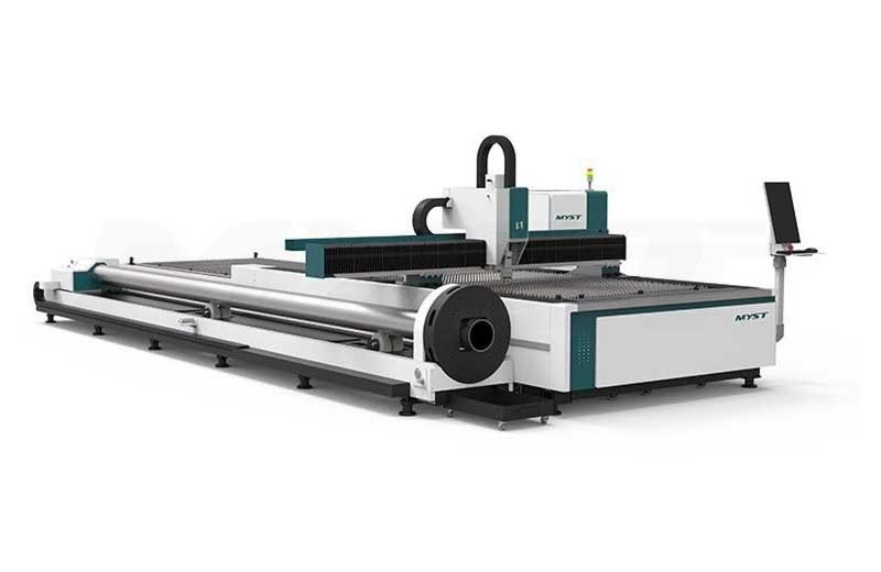
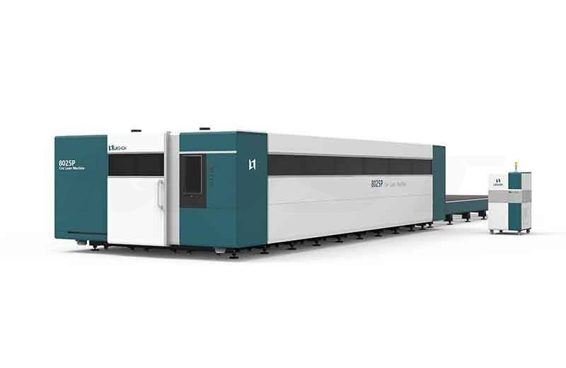
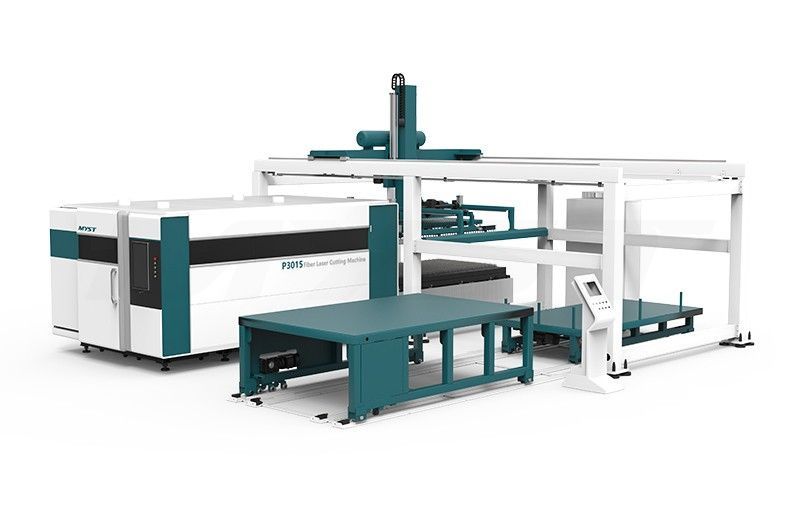
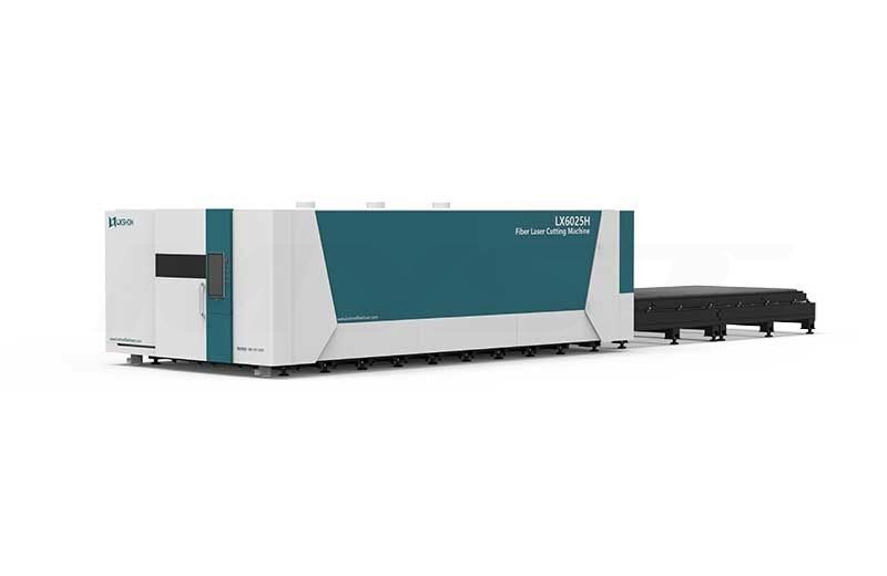
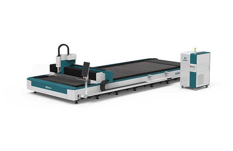
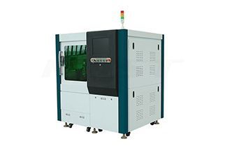
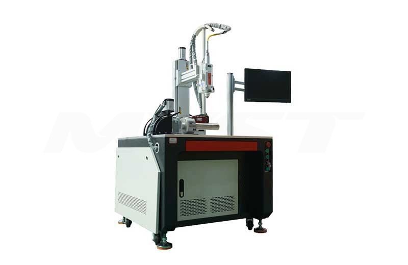
After analyzing the customer's process problems, MYST lasers recommend customers to use laser cutting, which is focused by the laser beam through the lens, and is concentrated into a very small spot at the focus, which can reach several micrometers and a few micrometers, and the focus is modulated. In the plane of the workpiece, when a beam of sufficient power is irradiated onto the object, the light energy is rapidly converted into heat energy, which will generate a local high temperature above 10000 °C to instantly melt or even vaporize the workpiece, thereby cutting the workpiece to the depth or cut through.

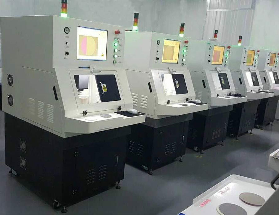
Through MYST's continuous efforts and equipment upgrades, we have successfully replaced the blade cutting equipment with laser cutting, which can meet the customer's GPP chip produced by electrophoresis, photoresist and knife scraping, which not only improves the cutting efficiency but also saves the cost. Promote the improvement of overall efficiency.


